October 8, 2019
Yale News (October 7, 2019), ‘Picoscience’ and a plethora of new materials
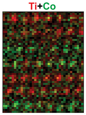
Yale researchers in “picoscience” are working to design and fabricate materials at the picometer scale — which is a million times smaller than a micrometer.

Yale News (October 7, 2019), ‘Picoscience’ and a plethora of new materials
Yale researchers in “picoscience” are working to design and fabricate materials at the picometer scale — which is a million times smaller than a micrometer.